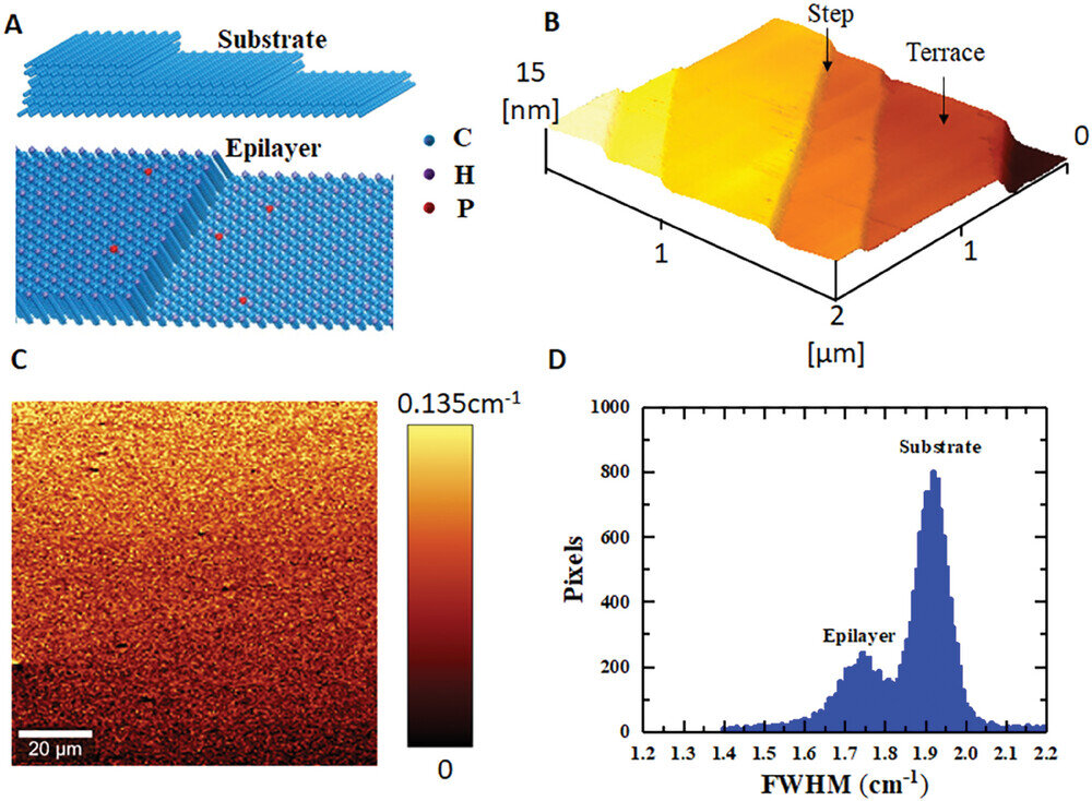
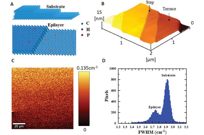
A research team from the National Institute for Materials Science has developed the world’s first n-channel diamond MOSFET, paving the way for harsh environment applications and diamond power electronics. The device’s development is a critical step towards CMOS integrated circuits. The research highlights the excellent thermal properties and energy efficiency of semiconductor diamond, which can operate under extreme conditions.
Main Points
World’s first n-channel diamond MOSFET
The world’s first n-channel diamond MOSFET developed by the NIMS research team offers a breakthrough in CMOS integrated circuits design for harsh environments, including high-performance and high-reliability applications.
Unique properties of semiconductor diamond
Semiconductor diamond’s unique properties such as ultra wide-bandgap energy, high carrier mobilities, and high thermal conductivity make it suitable for extreme environmental conditions.
Significance of diamond MOSFETs in electronics development
The development of n-channel diamond MOSFETs is a critical step towards the establishment of diamond CMOS devices, facilitating the creation of energy-efficient power electronics, spintronic devices, and MEMS sensors.
Insights
Diamond MOSFETs can withstand extreme environmental conditions
The n-channel diamond MOSFET’s development signifies an advancement in technology, enabling operations in harsh environments such as high temperatures and radiation levels, beneficial for areas like nuclear reactor cores.
Advancement in diamond electronics enhances energy efficiency
Using diamond electronics contributes to more energy-efficient devices capable of managing better in severe conditions, addressing the limitations of conventional semiconductors.
Links
- TechXplore article on World's first N-channel diamond field-effect transistor for CMOS integrated circuits
- Research published in Advanced Science
Images
URL
https://techxplore.com/news/2024-03-world-channel-diamond-field-effect.html